Jian Tang Lab
1. Topological quantum materials
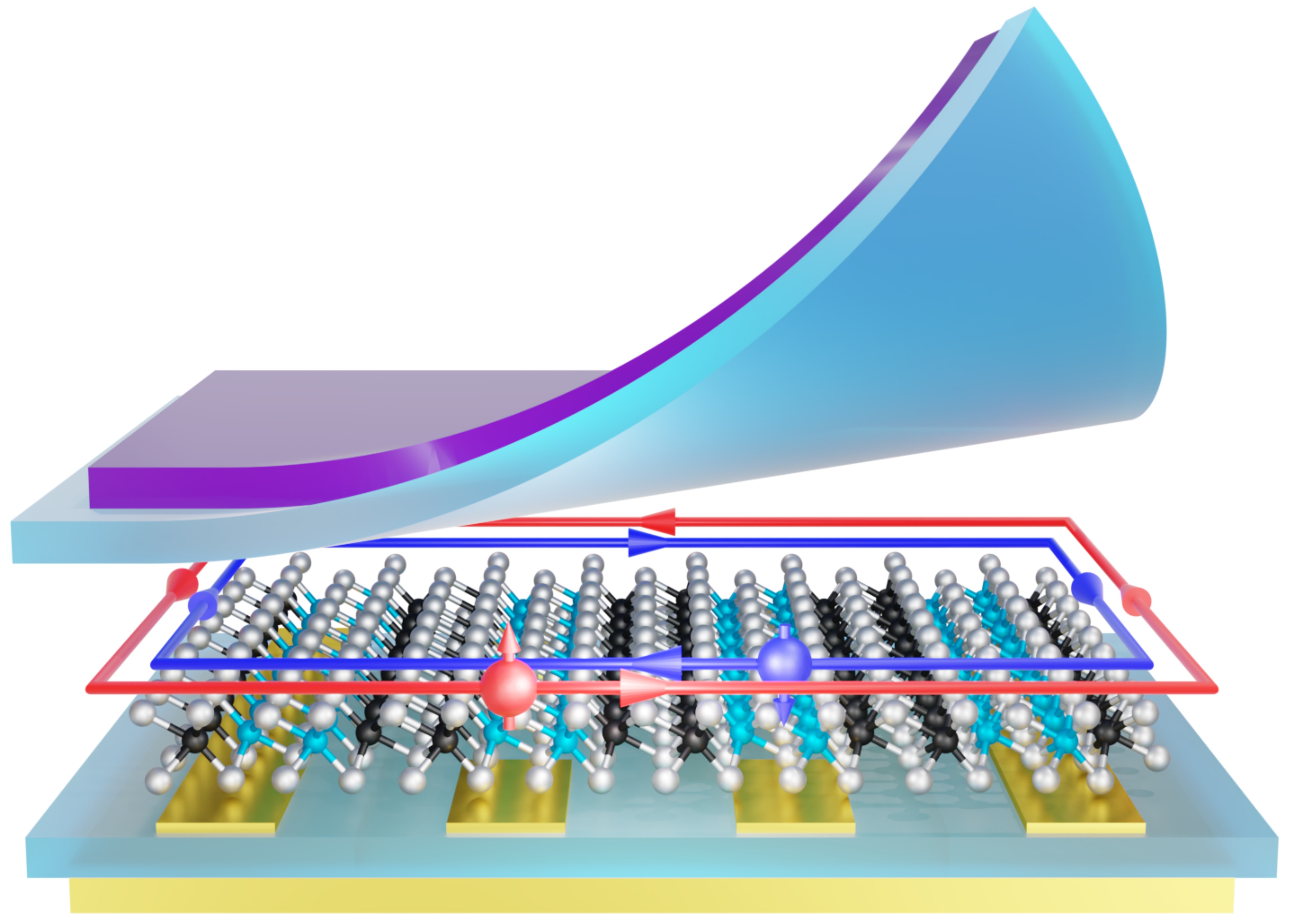
We explore the frontier where topology intersects with electron correlations in low-dimensional quantum materials and van der Waals heterostructures. By tuning electrostatic gating, layer stacking, twist angle, and proximity to ferromagnets or superconductors, we create and probe new quantum states arising from the interplay of symmetry, topology, electron interactions, lattice instabilities, and electron-phonon coupling, etc. Our goal is to uncover novel topological and correlated phases and to advance the understanding and control of emergent phenomena in a series of new quantum materials.
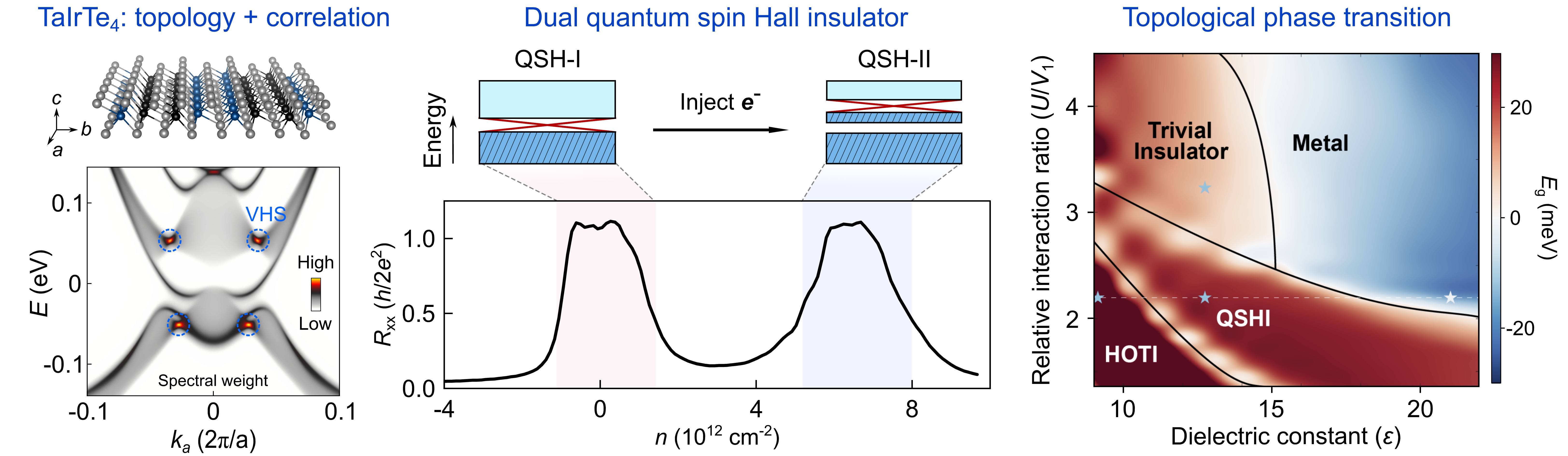
(1) For instance, we recently discovered a dual quantum spin Hall insulator in monolayer TaIrTe4 (Nature 628, 515, 2024), arising from the interplay of its single-particle topology and density-tuned electron correlations close to low-energy van Hove singularities. The discovery of the dual QSH insulator introduces a new method for creating topological flat minibands through CDW superlattices, which offer a promising platform for exploring time-reversal-symmetric fractional phases. Moreover, we further uncovered the interaction-driven topological phase transition (Phys. Rev. X, 2026) from a quantum spin Hall insulator to a trivial insulator, a higher-order topological insulator, and a metallic phase.
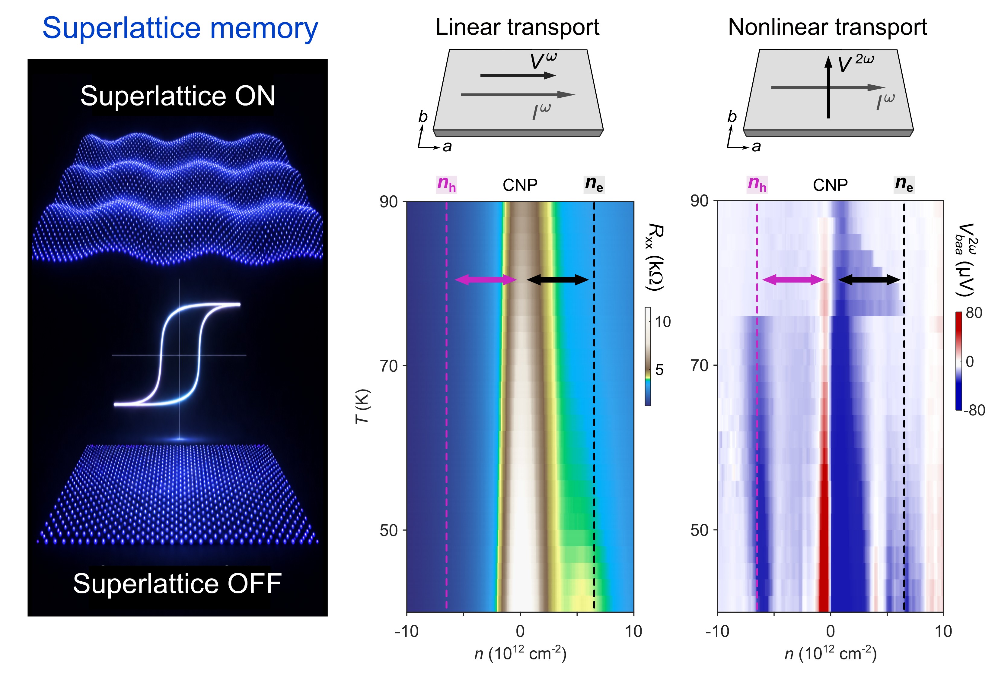
(2) Memory in materials is typically stored in charge or spin, as in ferroelectric and ferromagnetic systems. In monolayer TaIrTe4, we recently discovered a different possibility: memory encoded directly in the crystal lattice. A pristine monolayer can spontaneously develop a long-period superlattice upon "finite carrier doping and cooling" process. This superlattice can be electrically switched ON and OFF and remains stable after the field is removed — a nonvolatile spontaneous superlattice memory effect (Nature 652, 68, 2026). The switching toggles the system between two structural configurations whose unit-cell areas differ by nearly two orders of magnitude.
This phenomenon arises from the interplay between lattice and QSH electronic instabilities, revealed through complementary probes including linear and nonlinear transport measurements, Raman spectroscopy, and STM. Switching the superlattice simultaneously reshapes the electronic topology, enabling control of topological flat bands and correlated electronic states. More broadly, this spontaneous superlattice memory effect suggests a new direction for quantum materials: programmable superlattices as an active handle to control topological and electronic correlated phases.
2. 2D electronics: materials growth, device engineering, and integrated functional systems
Atomically thin two-dimensional (2D) materials provide a versatile platform for future electronics, owing to their exceptional electrical and mechanical properties, as well as their compatibility with aggressive scaling and heterogeneous integration. Realizing their full potential, however, requires coordinated advances in material synthesis, interface engineering, device fabrication, and system-level functionality.
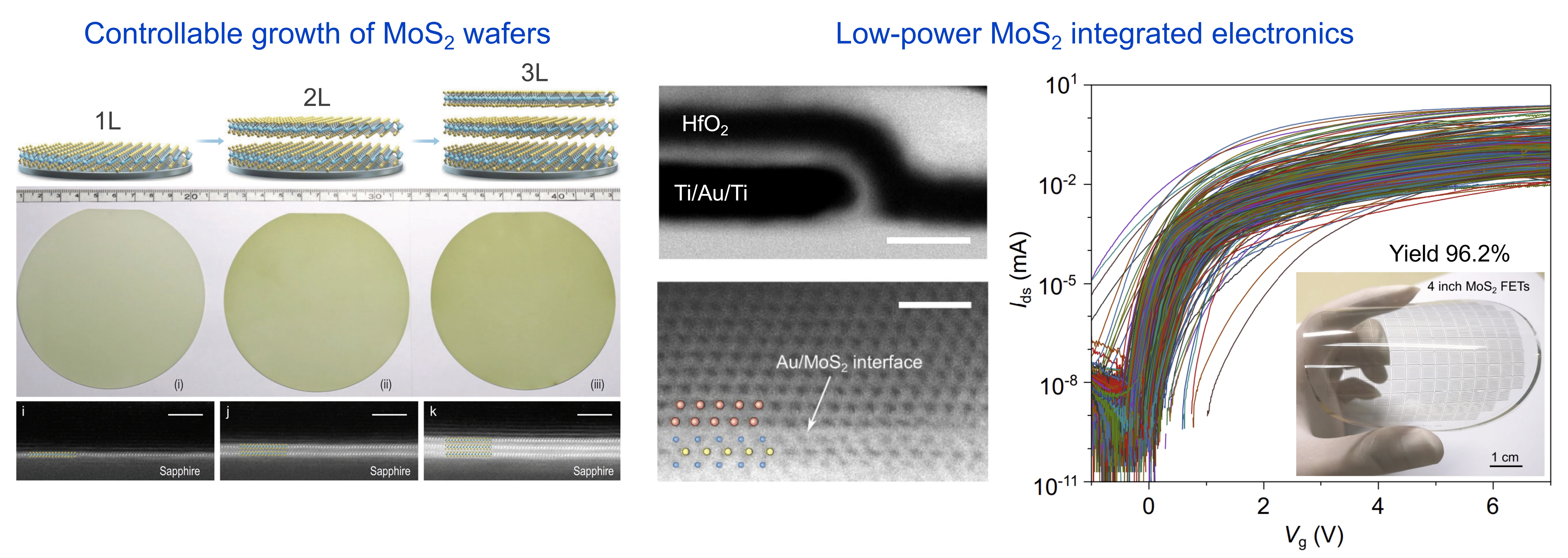
(1) We developed controllable epitaxial growth of high-quality MoS2 wafers by chemical vapor deposition, achieving domain sizes above 100 μm, excellent crystalline quality, tunable layer numbers (1L–3L) and stacking configurations, as well as controlled oxygen doping (Nano Lett. 2020; Small 2020; Natl. Sci. Rev. 2022).
(2) Building on this materials platform, we established key device technologies, including ultrathin high-κ dielectric integration (5 nm HfO2 with an equivalent oxide thickness of ~1 nm) and ohmic contacts with atomically sharp interfaces (Rc < 0.6 kΩ·μm). These advances enabled high-performance MoS2 thin-film transistors and large-scale flexible integrated logic circuits operating at low voltage (~0.5 V) and low power consumption (Nat. Commun. 2023).
(3) Beyond individual devices, we further explore how 2D materials can enable compact and multifunctional electronic systems. Taking advantage of their atomically thin nature and weak interlayer coupling, we investigated vertical integration of field-effect transistors with up to three device tiers and 16 van der Waals layers. We also demonstrated the integration of multiple functional layers, including all-2D floating-gate memory, logic computing, and optical sensing units, establishing a pathway toward three-dimensional, energy-efficient electronic architectures (Adv. Electron. Mater. 2020). In addition, by leveraging the multistate memory behavior of floating-gate devices, we developed artificial synaptic transistors for neuromorphic computing applications( Adv. Funct. Mater. 2021). Together, these efforts connect controllable material growth with functional device innovation, advancing both the fundamental and technological frontiers of 2D electronics.